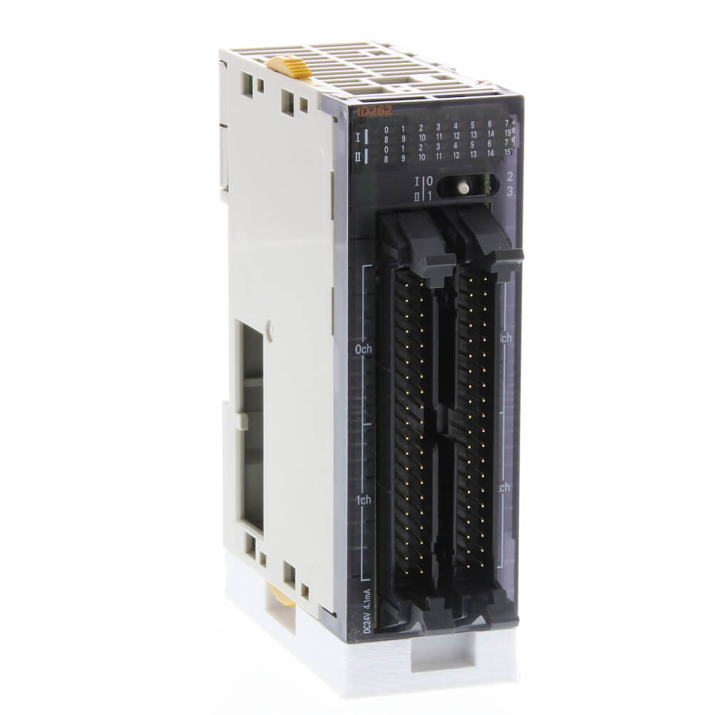
CJ1W-ID262 DC Input Unit (24 VDC, 64 Points)
| Name | 64-point DC Input Unit | |
|---|---|---|
| Model | CJ1W-ID262 | |
| Rated Input Voltage | 24 VDC | |
| Rated Input Voltage Range | 20.4 to 26.4 VDC | |
| Input Impedance | 5.6 kΩ | |
| Input Current | 4.1 mA typical (at 24 VDC) | |
| ON Voltage/ON Current | 19.0 VDC min./3 mA min. | |
| OFF Voltage/OFF Current | 5 VDC max./1 mA max. | |
| ON Response Time | 8.0 ms max. (Can be set to between 0 and 32 in the Setup.) * | |
| OFF Response Time | 8.0 ms max. (Can be set to between 0 and 32 in the Setup.) * | |
| Number of Circuits | 64 (16 points/common, 4 circuits) | |
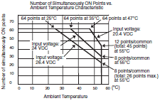
| Number of Simultaneously ON Points |
50% (8 points/common) simultaneously ON (at 24 VDC) (Refer to the following illustrations.) | |
| Insulation Resistance | 20 MΩ min. between external terminals and the GR terminal (100 VDC) | |
| Dielectric Strength | 1,000 VAC between the external terminals and the GR terminal for 1 minute at a leakage current of 10 mA max. |
|
| Internal Current Consumption | 90 mA max. | |
| Weight | 110 g max. | |
| Accessories | None | |
| Circuit Configuration |
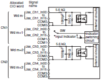 The signal names of the terminals are the device variable names. The device variable names are the names that use “Jxx” as the device name. |
 |
| External connection and terminal-device variable diagram |
CN1 | CN2 |
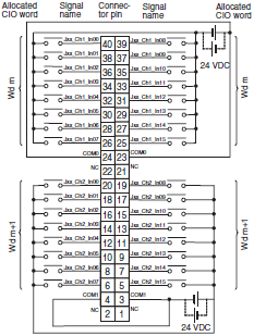 The input power polarity can be connected in either direction. Be sure to wire both pins 23 and 24 (COM0) of CN1, and set the same polarity for both pins. Be sure to wire both pins 3 and 4 (COM1) of CN1, and set the same polarity for both pins. The signal names of the terminals are the device variable names. The device variable names are the names that use “Jxx” as the device name. |
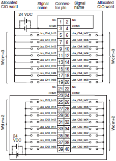 The input power polarity can be connected in either direction. Be sure to wire both pins 23 and 24 (COM2) of CN2, and set the same polarity for both pins. Be sure to wire both pins 3 and 4 (COM3) of CN2, and set the same polarity for both pins. The signal names of the terminals are the device variable names. The device variable names are the names that use “Jxx” as the device name. |
|
* The ON response time will be 120 μs maximum and OFF response time will be 400 μs maximum even if the response
times are set to 0 ms due to internal element delays.
Note: Observe the following restrictions when connecting to a 2-wire sensor.
• Make sure the input power supply voltage is larger than the ON voltage (19 V) plus the residual voltage of the
sensor (approx. 3 V).
• Use a sensor with a minimum load current of 3 mA min.
• Connect bleeder resistance if you connect a sensor with a minimum load current of 5 mA or higher.
times are set to 0 ms due to internal element delays.
Note: Observe the following restrictions when connecting to a 2-wire sensor.
• Make sure the input power supply voltage is larger than the ON voltage (19 V) plus the residual voltage of the
sensor (approx. 3 V).
• Use a sensor with a minimum load current of 3 mA min.
• Connect bleeder resistance if you connect a sensor with a minimum load current of 5 mA or higher.